Article
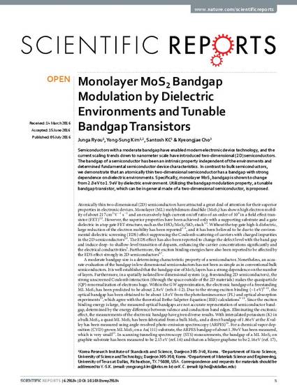
Monolayer MoS2 Bandgap Modulation by Dielectric Environments and Tunable Bandgap Transistors
Scientific Reports
(2016)
Abstract
Semiconductors with a moderate bandgap have enabled modern electronic device technology, and the current scaling trends down to nanometer scale have introduced two-dimensional (2D) semiconductors. The bandgap of a semiconductor has been an intrinsic property independent of the environments and determined fundamental semiconductor device characteristics. In contrast to bulk semiconductors, we demonstrate that an atomically thin two-dimensional semiconductor has a bandgap with strong dependence on dielectric environments. Specifically, monolayer MoS2 bandgap is shown to change from 2.8 eV to 1.9 eV by dielectric environment. Utilizing the bandgap modulation property, a tunable bandgap transistor, which can be in general made of a two-dimensional semiconductor, is proposed.
Disciplines
Publication Date
July 5, 2016
DOI
10.1038/srep29184
Publisher Statement
SJSU users: Use the following link to login and access the article via SJSU databases.
This article was published in Scientific Reports, volume 6, 2016, and can also be found online here.
Copyright © 2016, The Authors
Citation Information
Junga Ryou, Yong-Sung Kim, Santosh KC and Kyeongjae Cho. "Monolayer MoS2 Bandgap Modulation by Dielectric Environments and Tunable Bandgap Transistors" Scientific Reports Vol. 6 (2016) Available at: http://works.bepress.com/santosh-kc/7/
Creative Commons license

This work is licensed under a Creative Commons CC_BY International License.