
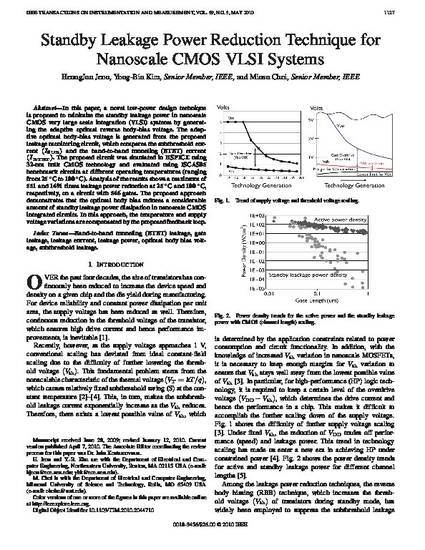
In this paper, a novel low-power design technique is proposed to minimize the standby leakage power in nanoscale CMOS very large scale integration (VLSI) systems by generating the adaptive optimal reverse body-bias voltage. The adaptive optimal body-bias voltage is generated from the proposed leakage monitoring circuit, which compares the subthreshold current (ISUB) and the band-to-band tunneling (BTBT) current (IBTBT). The proposed circuit was simulated in HSPICE using 32-nm bulk CMOS technology and evaluated using ISCAS85 benchmark circuits at different operating temperatures (ranging from 25°C to 100°C). Analysis of the results shows a maximum of 551 and 1491 times leakage power reduction at 25°C and 100°C, respectively, on a circuit with 546 gates. The proposed approach demonstrates that the optimal body bias reduces a considerable amount of standby leakage power dissipation in nanoscale CMOS integrated circuits. In this approach, the temperature and supply voltage variations are compensated by the proposed feedback loop.
- Band-To-Band Tunneling (BTBT) Leakage,
- Gate Leakage,
- Leakage Current,
- Leakage Power,
- Optimal Body Bias Voltage,
- Subthreshold Leakage,
- Band to Band Tunneling,
- Body Bias,
- Sub-Threshold Leakage,
- Bias Voltage,
- CMOS Integrated Circuits,
- Electric Network Analysis,
- Nanostructured Materials,
- Optimization,
- Standby Power Systems,
- Tunneling (Excavation),
- Wind Tunnels
Available at: http://works.bepress.com/minsu-choi/100/