
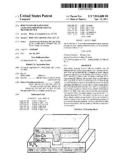
Non-volatile memory devices with two stacked layers of chalcogenide materials comprising the active memory device have been investigated for their potential as phase change memories. The devices tested included GeTe/SnTe, Ge2Se3/SnTe, and Ge2Se3/SnSe stacks. All devices exhibited resistance switching behavior. The polarity of the applied voltage with respect to the SnTe or SnSe layer was critical to the memory switching properties, due to the electric field induced movement of either Sn or Te into the Ge-chalcogenide layer. One embodiment of the invention is a device comprising a stack of chalcogenide-containing layers which exhibit phase change switching only after a reverse polarity voltage potential is applied across the stack causing ion movement into an adjacent layer and thus "activating" the device to act as a phase change random access memory device or a reconfigurable electronics device when the applied voltage potential is returned to the normal polarity. Another embodiment of the invention is a device that is capable of exhibiting more that two data states.
Available at: http://works.bepress.com/kris_campbell/25/
20 Claims, 12 Drawing Sheets