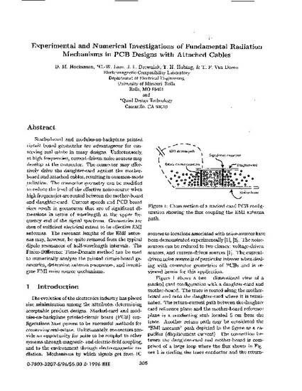
Stacked-card and modules-on-backplane printed circuit board geometries are advantageous for conserving real-estate in many designs. Unfortunately, at high frequencies, current-driven noise sources may develop at the connector. The connector may effectively drive the daughter-card against the motherboard and attached cables, resulting in common-mode radiation. The connector geometry can be modified to reduce the level of the effective noise-source when high frequencies are routed between the mother-board and daughter-card. Current speeds and PCB board sizes result in geometries that are of significant dimensions in terms of wavelength at the upper frequency end of the signal spectrum. Geometries are then of sufficient electrical extent to be effective EMI antennas. The resonant lengths of the EMI antennas may, however, be quite removed from the typical dipole resonances of half-wavelength intervals. The Finite-Difference Time-Domain method can be used to numerically analyze the printed circuit-board geometries, determine antenna resonances, and investigate EMI noise source mechanisms.
- EMI Antennas,
- EMI Noise Source Mechanisms,
- PCB Designs,
- Add-On Boards,
- Antenna Resonances,
- Attached Cables,
- Common-Mode Radiation,
- Connector,
- Current-Driven Noise Sources,
- Daughter-Card,
- Dipole Resonances,
- Electric Connectors,
- Finite Difference Time-Domain Analysis,
- Finite-Difference Time-Domain Method,
- Fundamental Radiation Mechanisms,
- Modules-On-Backplane Printed Circuit Board Geometries,
- Motherboard,
- Printed Circuit Design,
- Printed Circuit-Board Geometries,
- Radiofrequency Interference,
- Resonant Lengths,
- Stacked-Card Printed Circuit Board Geometries
Available at: http://works.bepress.com/james-drewniak/135/
