
Article
Infiltration and Inversion of Holographically Defined Polymer Photonic Crystal Templates by Atomic Layer Deposition
Advanced Materials
(2006)
Abstract
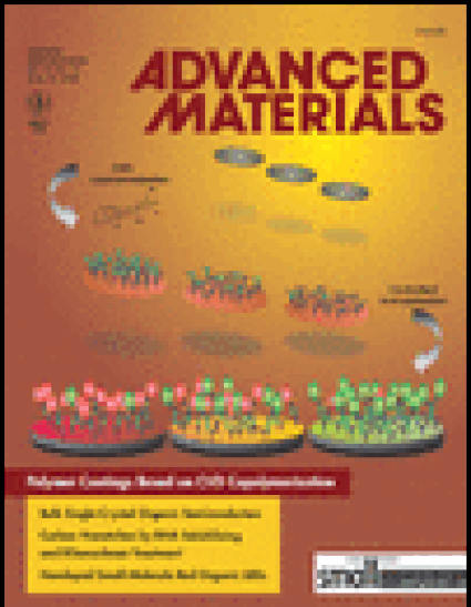
Practical methods of microfabrication are vital for the development of photonic-crystal-based signal processing. However, extension of the optical methods that dominate integrated circuit fabrication to three dimensions is challenging. This communication reports an essential step for creation of devices operating within a full photonic band gap: atomic layer deposition is used to create the high-index TiO2 replicas of holographically defined photonic crystals shown in the figure.
Keywords
- Atomic layer deposition,
- Chemical vapor deposition,
- Holography,
- Photonic crystals,
- Two-photon absorption
Disciplines
Publication Date
June 1, 2006
Citation Information
Jeffrey S. King, Elton Graugnard, Olivia M. Roche, David N. Sharp, et al.. "Infiltration and Inversion of Holographically Defined Polymer Photonic Crystal Templates by Atomic Layer Deposition" Advanced Materials Vol. 18 Iss. 12 (2006) Available at: http://works.bepress.com/elton_graugnard/21/