
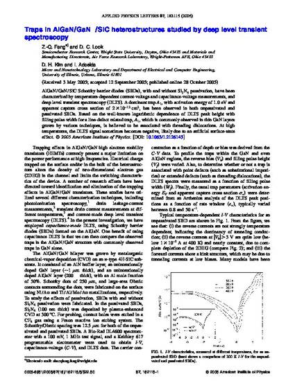
AlGaN/GaN/SiC Schottky barrier diodes (SBDs), with and without Si3N4 passivation, have been characterized by temperature-dependent current-voltage and capacitance-voltage measurements, and deep level transient spectroscopy (DLTS). A dominant trap A1, with activation energy of 1.0 eV and apparent capture cross section of 2×10⁻¹² cm2, has been observed in both unpassivated and passivated SBDs. Based on the well-known logarithmic dependence of DLTS peak height with filling pulse width for a line-defect related trap, A1, which is commonly observed in thin GaN layers grown by various techniques, is believed to be associated with threading dislocations. At high temperatures, the DLTS signal sometimes becomes negative, likely due to an artificial surface-state effect.
Available at: http://works.bepress.com/david_look/86/
Copyright © 2005, American Institute of Physics. This article may be downloaded for personal use only. Any other use requires prior permission of the author and the American Institute of Physics. The following article appeared in Applied Physics Letters 87.18, and may be found at http://apl.aip.org/applab/v87/i18/p182115_s1