
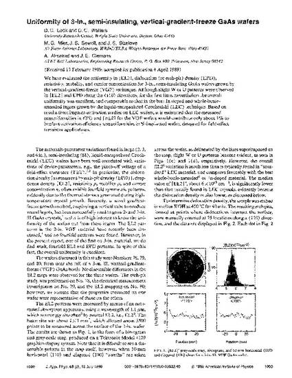
We have evaluated the uniformity in [EL2], dislocation (or etch‐pit) density (EPD), resistivity, mobility, and carrier concentration for 3‐in., semi‐insulating GaAs wafers grown by the vertical‐gradient‐freeze (VGF) technique. Although slight W or U patterns were observed in [EL2] and EPD along the 〈110〉 directions, for the first time, nevertheless the overall uniformity was excellent, and comparable to that in the best In‐doped and whole‐boule‐annealed ingots grown by the liquid‐encapsulated Czochralski (LEC) technique. Based on results from implant‐activation studies on LEC wafers, it is estimated that the measured nonuniformities in EPD and [EL2] for the VGF wafers would contribute only about 1% to implant‐activation‐efficiency nonuniformities in Si‐implanted wafers designed for field‐effect transistor applications.
Available at: http://works.bepress.com/david_look/80/
Copyright © 1989, American Institute of Physics. This article may be downloaded for personal use only. Any other use requires prior permission of the author and the American Institute of Physics. The following article appeared in the Journal of Applied Physics 66.2, and may be found at http://jap.aip.org/resource/1/japiau/v66/i2/p1000_s1