Article
Deep-Center Hopping Conduction in GaN
Journal of Applied Physics
Document Type
Article
Publication Date
9-1-1996
Disciplines
Abstract
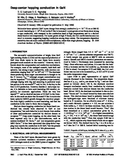
Molecular‐beam‐epitaxial GaN layers change from strongly conductive (ρ≂10−2 Ω cm at 300 K) to semi‐insulating (ρ≂106 Ω cm) as the N flux is increased. Layers grown at low fluxes show strong n‐type conduction, with transport in the conduction band at high temperatures and in a shallow donor band at low temperatures. For layers grown at high N fluxes, the Hall coefficients become too small to measure, suggesting hopping conduction among deep centers. The temperature‐dependent resistivity data are most consistent with multiphonon, rather than single‐phonon, hopping.
DOI
10.1063/1.363128
Citation Information
David C. Look, D. C. Reynolds, W. Kim, Ö. Aktas, et al.. "Deep-Center Hopping Conduction in GaN" Journal of Applied Physics Vol. 80 Iss. 5 (1996) p. 2960 - 2963 ISSN: 0021-8979 Available at: http://works.bepress.com/david_look/74/

Copyright © 1996, American Institute of Physics. This article may be downloaded for personal use only. Any other use requires prior permission of the author and the American Institute of Physics. The following article appeared in the Journal of Applied Physics 80.5, and may be found at http://jap.aip.org/resource/1/japiau/v80/i5/p2960_s1