
Article
Characterization of Near-Surface Traps in Semiconductors: GaN
Applied Physics Letters
Document Type
Article
Publication Date
7-1-2001
Disciplines
Abstract
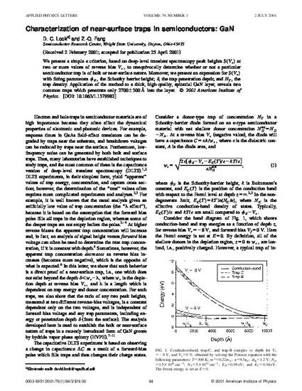
We present a simple a criterion, based on deep-level transient spectroscopy peak heights S(Vr) at two or more values of reverse bias Vr, to unequivocally determine whether or not a particular semiconductor trap is of bulk or near-surface nature. Moreover, we present an expression for S(Vr) with fitting parameters ϕB, the Schottky barrier height; δ, the trap penetration depth; and NT, the trap density. Application of the method to a thick, high-quality, epitaxial GaN layer, reveals two common traps which penetrate only 2700±300 Å into the layer.
DOI
10.1063/1.1379982
Citation Information
David C. Look and Z-Q. Fang. "Characterization of Near-Surface Traps in Semiconductors: GaN" Applied Physics Letters Vol. 79 Iss. 1 (2001) p. 84 - 86 ISSN: 0003-6951 Available at: http://works.bepress.com/david_look/59/
Copyright © 2001, American Institute of Physics. This article may be downloaded for personal use only. Any other use requires prior permission of the author and the American Institute of Physics. The following article appeared in Applied Physics Letters 79.1, and may be found at http://apl.aip.org/resource/1/applab/v79/i1/p84_s1