
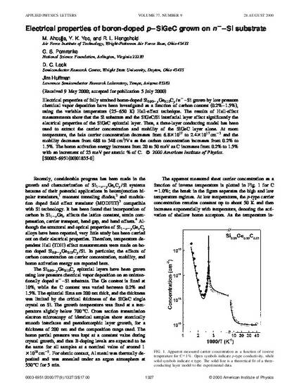
Electrical properties of fully strained boron-doped Si0.90−yGe0.10Cy/n−–Si grown by low pressure chemical vapor deposition have been investigated as a function of carbon content (0.2%–1.5%), using the variable temperature (25–650 K) Hall-effect technique. The results of Hall-effect measurements show that the Si substrate and the SiGeC/Si interfacial layer affect significantly the electrical properties of the SiGeC epitaxial layer. Thus, a three-layer conducting model has been used to extract the carrier concentration and mobility of the SiGeC layer alone. At room temperature, the hole carrier concentration decreases from 6.8×10¹⁷ to 2.4×1017 cm−3 and the mobility decreases from 488 to 348 cm2/V s as the carbon concentration increases from 0.2% to 1.5%. The boron activation energy increases from 20 to 50 meV as C increases from 0.2% to 1.5% with an increment of 23 meV per atomic % of C.
Available at: http://works.bepress.com/david_look/26/
Copyright © 2000, American Institute of Physics. This article may be downloaded for personal use only. Any other use requires prior permission of the author and the American Institute of Physics. The following article appeared in Applied Physics Letters 77.9, and may be found at http://apl.aip.org/resource/1/applab/v77/i9/p1327_s1