Article
Effects of in Profile on Material and Device Properties of AlGaAs/InGaAs/GaAs High Electron Mobility Transistors
Journal of Applied Physics
Document Type
Article
Publication Date
1-1-1996
Disciplines
Abstract
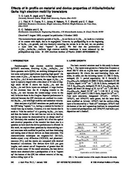
The molecular‐beam‐epitaxial growth of InxGa1−xAs on GaAs or AlyGa1−yAs leads to a variation of In content with depth, due to In segregation. However, by predepositing In at the beginning of InxGa1−xAs growth, and also thermally removing the excess In at the end, we can produce a layer with the ideal ‘‘square’’ In profile. We find that the performance of AlyGa1−yAs/InxGa1−xAs/GaAs high electron mobility transistors is most enhanced by the predeposition step alone.
DOI
10.1063/1.360862
Citation Information
David C. Look, B. Jogai, R. Kaspi, J. L. Ebel, et al.. "Effects of in Profile on Material and Device Properties of AlGaAs/InGaAs/GaAs High Electron Mobility Transistors" Journal of Applied Physics Vol. 79 Iss. 1 (1996) p. 540 - 544 ISSN: 0021-8979 Available at: http://works.bepress.com/david_look/20/

Copyright © 1996, American Institute of Physics. This article may be downloaded for personal use only. Any other use requires prior permission of the author and the American Institute of Physics. The following article appeared in the Journal of Applied Physics 79.1, and may be found at http://jap.aip.org/resource/1/japiau/v79/i1/p540_s1