Article
Origin of Conductive Surface Layer in Annealed ZnO
Applied Physics Letters
Document Type
Article
Publication Date
1-1-2008
Disciplines
Abstract
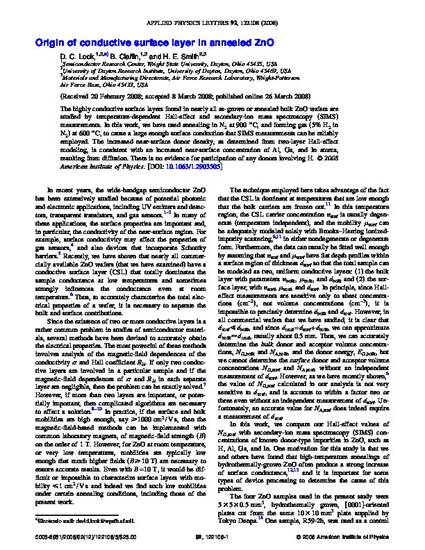
The highly conductive surface layers found in nearly all as-grown or annealed bulk ZnO wafers are studied by temperature-dependent Hall-effect and secondary-ion mass spectroscopy (SIMS) measurements. In this work, we have used annealing in N2 at 900 degrees C, and forming gas (5% H2 in N2) at 600 degrees C, to cause a large enough surface conduction that SIMS measurements can be reliably employed. The increased near-surface donor density, as determined from two-layer Hall-effect modeling, is consistent with an increased near-surface concentration of Al, Ga, and In atoms, resulting from diffusion. There is no evidence for participation of any donors involving H.
DOI
10.1063/1.2903505
Citation Information
David C. Look, B. Claflin and Helen Smith. "Origin of Conductive Surface Layer in Annealed ZnO" Applied Physics Letters Vol. 92 Iss. 12 (2008) ISSN: 0003-6951 Available at: http://works.bepress.com/david_look/192/

Copyright © 2008, American Institute of Physics. This article may be downloaded for personal use only. Any other use requires prior permission of the author and the American Institute of Physics. The following article appeared in Applied Physics Letters 92.12, and may be found at http://apl.aip.org/