Article
Nondestructive Mapping of Carrier Concentration and Dislocation Density in N(+)-Type GaAs
Applied Physics Letters
Document Type
Article
Publication Date
10-1-1994
Disciplines
Abstract
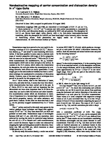
Transmission mappings (500 μm×500 μm resolution) at wavelengths of 0.9–1.5 μm on 3 in., n+‐GaAs wafers (n≂1–2×1018 cm-3) correlate well with carrier concentration n, measured by the Hall effect, and dislocation density, as confirmed by KOH etch‐pit patterns. The absorption for λ≳1.0 μm (below band edge) varies directly with n via free‐carrier interconduction‐band transitions, while the absorption for λ≲0.95 μm (near band edge) varies inversely with n because of band‐filling effects. Both phenomena are highly useful for n+‐GaAs wafer characterization.
DOI
10.1063/1.112757
Citation Information
David C. Look, D. C. Walters, M. G. Mier and J. R. Sizelove. "Nondestructive Mapping of Carrier Concentration and Dislocation Density in N(+)-Type GaAs" Applied Physics Letters Vol. 65 Iss. 17 (1994) p. 2188 - 2190 ISSN: 0003-6951 Available at: http://works.bepress.com/david_look/18/

Copyright © 1994, American Institute of Physics. This article may be downloaded for personal use only. Any other use requires prior permission of the author and the American Institute of Physics. The following article appeared in Applied Physics Letters 65.17, and may be found at http://apl.aip.org/resource/1/applab/v65/i17/p2188_s1