Article
Deviations from Bulk Transport Measurements in Semi-Insulating GaAs
Journal of Applied Physics
Document Type
Article
Publication Date
11-1-1989
Disciplines
Abstract
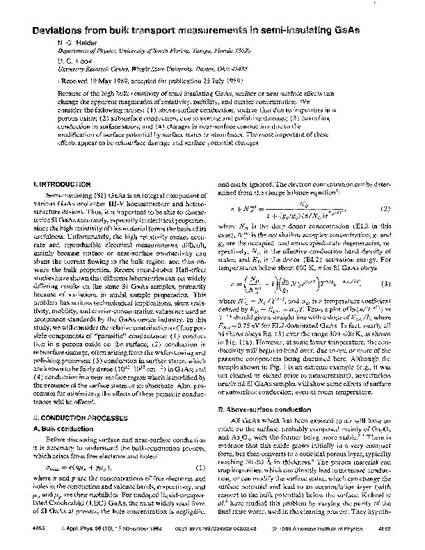
Because of the high bulk resistivity of semi‐insulating GaAs, surface or near‐surface effects can change the apparent magnitudes of resistivity, mobility, and carrier concentration. We consider the following causes: (1) above‐surface conduction, such as that due to impurities in a porous oxide; (2) subsurface conduction, due to sawing and polishing damage; (3) tunneling conduction in surface states; and (4) changes in near‐surface conduction due to the modification of surface potential by surface states or absorbates. The most important of these effects appear to be subsurface damage and surface potential changes.
DOI
10.1063/1.343803
Citation Information
N. C. Halder and David C. Look. "Deviations from Bulk Transport Measurements in Semi-Insulating GaAs" Journal of Applied Physics Vol. 66 Iss. 10 (1989) p. 4858 - 4861 ISSN: 0021-8979 Available at: http://works.bepress.com/david_look/128/

Copyright © 1989, American Institute of Physics. This article may be downloaded for personal use only. Any other use requires prior permission of the author and the American Institute of Physics. The following article appeared in the Journal of Applied Physics 66.10, and may be found at http://jap.aip.org/resource/1/japiau/v66/i10/p4858_s1