Article
A New Technique for Whole-Wafer Etch-Pit Density Mapping in GaAs
Journal of Applied Physics
Document Type
Article
Publication Date
2-1-1989
Disciplines
Abstract
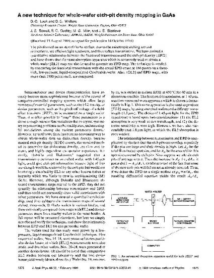
The pits formed on an etched GaAs surface, due to the anisotropic etching around dislocations, are efficient light scatterers, and thus reduce transmission. We have derived a quantitative relationship between the fractional transmission and the etch‐pit density (EPD) and have shown that the same absorption apparatus which is commonly used to obtain a whole‐wafer [EL2] map can also be used to generate an EPD map. The technique is verified by comparing the fractional transmission with the actual EPD count at 166 points on a three‐inch, low‐pressure, liquid‐encapsulated Czochralski wafer. Also, [EL2] and EPD maps, with more than 3500 points each, are compared.
DOI
10.1063/1.342984
Citation Information
David C. Look, D. C. Walters, J. S. Sewell, S. C. Dudley, et al.. "A New Technique for Whole-Wafer Etch-Pit Density Mapping in GaAs" Journal of Applied Physics Vol. 65 Iss. 3 (1989) p. 1375 - 1377 ISSN: 0021-8979 Available at: http://works.bepress.com/david_look/115/

Copyright © 1989, American Institute of Physics. This article may be downloaded for personal use only. Any other use requires prior permission of the author and the American Institute of Physics. The following article appeared in the Journal of Applied Physics 65.3, and may be found at http://jap.aip.org/resource/1/japiau/v65/i3/p1375_s1.