
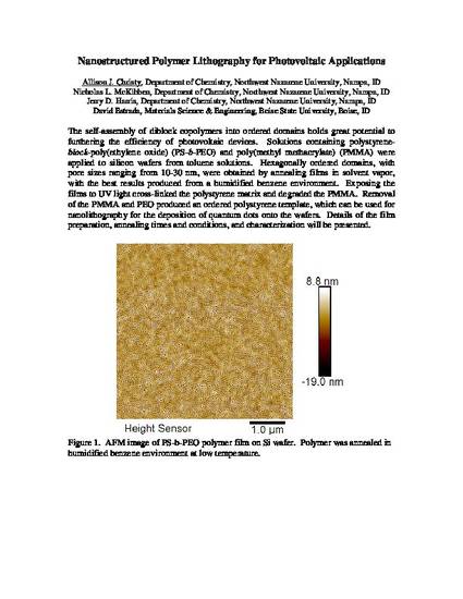
The self-assembly of diblock copolymers into ordered domains holds great potential to furthering the efficiency of photovoltaic devices. Solutions containing polystyrene-block-poly(ethylene oxide) (PS-b-PEO) and poly(methyl methacrylate) (PMMA) were applied to silicon wafers from toluene solutions. Hexagonally ordered domains, with pore sizes ranging from 10-30 nm, were obtained by annealing films in solvent vapor, with the best results produced from a humidified benzene environment. Exposing the films to UV light cross-linked the polystyrene matrix and degraded the PMMA. Removal of the PMMA and PEO produced an ordered polystyrene template, which can be used for nanolithography for the deposition of quantum dots onto the wafers. Details of the film preparation, annealing times and conditions, and characterization will be presented.
Available at: http://works.bepress.com/david_estrada/39/