
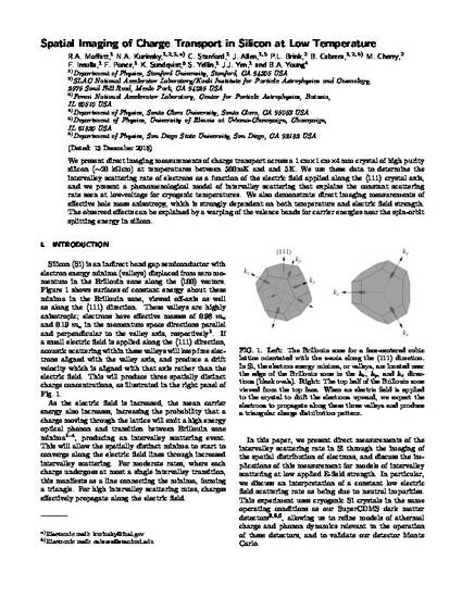
We present direct imaging measurements of charge transport across a 1 cm × 1 cm × 4 mm crystal of high purity silicon (∼20 kΩ cm) at temperatures between 500 mK and 5 K. We use these data to determine the intervalley scattering rate of electrons as a function of the electric field applied along the ⟨111⟩ crystal axis, and we present a phenomenological model of intervalley scattering which explains the constant scattering rate seen at low-voltage for cryogenic temperatures. We also demonstrate direct imaging measurements of effective hole mass anisotropy, which is strongly dependent on both temperature and electric field strength. The observed effects can be explained by a warping of the valence bands for carrier energies near the spin-orbit splitting energy in silicon.
Copyright © 2019 American Institute of Physics Publishing. Reprinted with permission.