
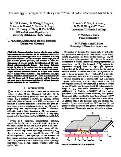
Because of the low electron effective mass and the high resulting carrier velocities, we are developing InGaAs/InP MOSFETs for potential application in VLSI circuits at scaling generations beyond 22 nm. We will report device design, review gate dielectric growth processes, and describe in detail the development of process modules for fabrication of fully self-aligned enhancement-mode devices. Key design challenges include the effect of the low density of states upon drive current and the effect of the low carrier mass on vertical confinement. Target electrical parameters include ~5 mA/μm drive current and ~7 mS/μm2 transconductance. Key fabrication challenges include formation of self-aligned N+ source and drain contacts with < 15 Ω-μm and < 1 Ω-μm2 resistivity, and the formation and patterning of the gate metal and dielectric without damage to the thin underlying 4–6 nm channel layer.
Available at: http://works.bepress.com/paul_simmonds/29/