Other
Method of manufacturing a semiconductor wafer level package, US Patent # 6,465,281
(2002)
Abstract
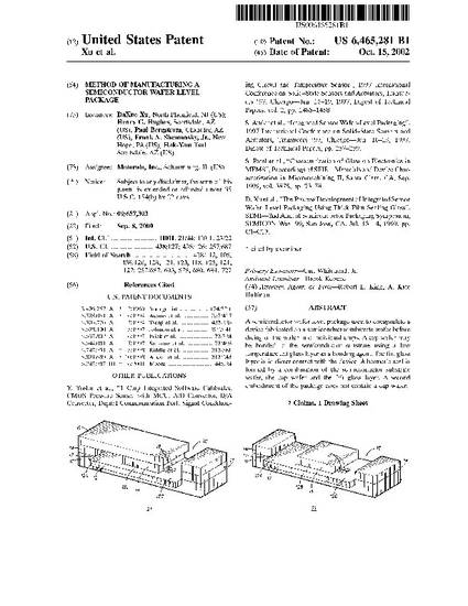
A semiconductor wafer level package used to encapsulate a device fabricated on a semiconductor substrate wafer before dicing of the wafer into individual chips. A cap wafer may be bonded to the semiconductor substrate using a low temperature frit glass layer as a bonding agent. The frit glass layer is in direct contact with the device. A hermetic seal is formed by a combination of the semiconductor substrate wafer, the cap wafer and the frit glass layer. A second embodiment of the package does not contain a cap wafer.
Disciplines
Publication Date
October, 2002
Comments
Assignee: Motorola, Inc., Schaumburg, IL (US)
Citation Information
DaXue Xu, Henry H. Hughes, Paul L. Bergstorm, Frank A. Shemansky, et al.. "Method of manufacturing a semiconductor wafer level package, US Patent # 6,465,281" (2002) Available at: http://works.bepress.com/paul-bergstrom/50/
